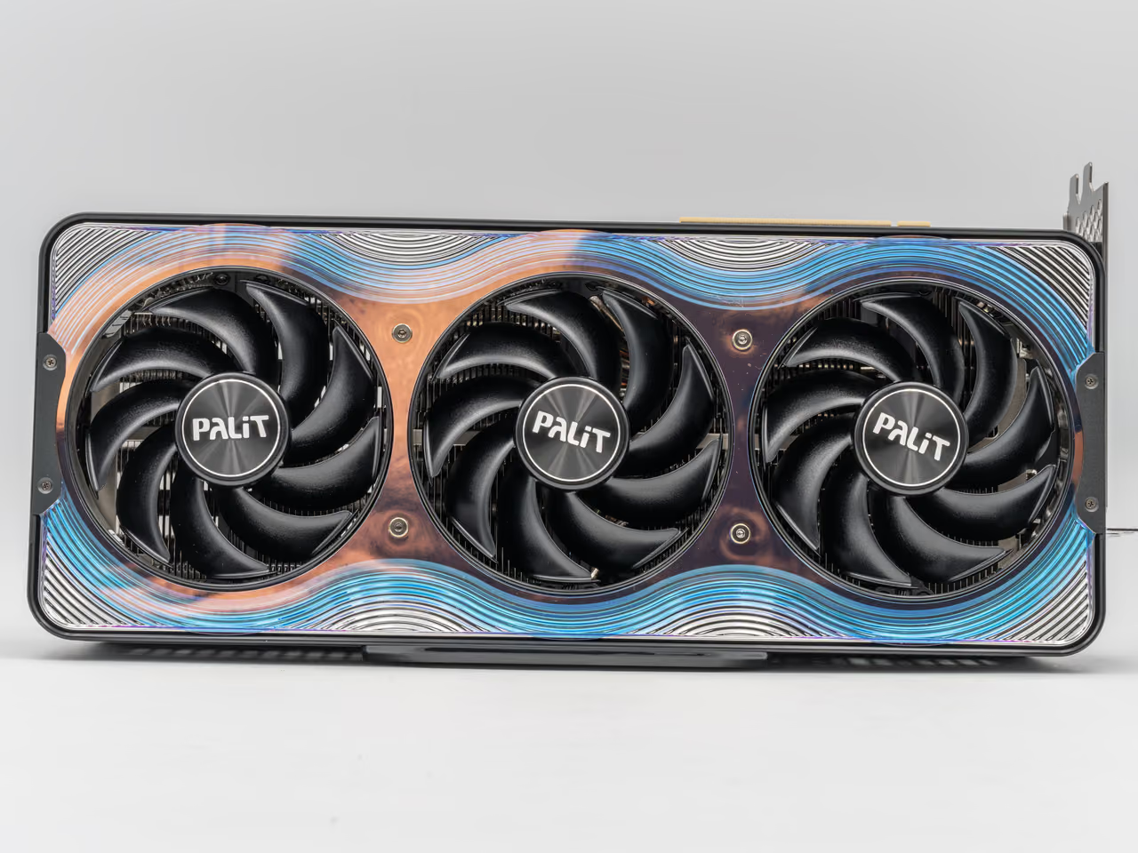
| Clock frequency gpu | 2.01 GHz | Confirmed | Vendor-rated | Nominal clock Stated by the vendorReference card, as specified in NVIDIA's product specification table. The base clock, from the product page: the whitepaper's appendix states only the boost clock. It is the figure that belongs beside a fixed frequency, and the reason a reader can put this card next to a Commodore 64 without the comparison quietly changing what it means. | |
| Clock frequency gpu | 2407 MHz | Confirmed | Vendor-rated | Peak clock Stated by the vendorReference card, the frequency NVIDIA guarantees the card reaches when power and thermal headroom allow. Taken from the whitepaper, which states 2407 MHz, rather than from the product page, which states 2.41 GHz. That is the same figure to three digits, and the more precise one is the one recorded. A ceiling reached when there is headroom, so it shares a comparability group with the GeForce GTX 1080's boost clock and with the PlayStation 5's variable-frequency maximum, and none with a fixed clock. | |
| Peak FP32 rate gpu | 104.8 TFLOP/s | Confirmed | Theoretical | Theoretical peak Stated by the vendor21 760 cores at the 2407 MHz boost clock, on the general shader units rather than the tensor cores. A theoretical peak, not an achieved rate. The whitepaper writes "Peak FP32 TFLOPS (non-Tensor)", which names both the precision and the units that produce it, so this rate is comparable with the GeForce GTX 1080's and with nothing else on the card. The product page's "3352 AI TOPS" and "318 TFLOPS" are not recorded anywhere in this catalog: the first counts low-precision tensor operations, the second is the ray-tracing engine's, and neither may be divided by a single-precision peak. | |
| Geekbench Compute score, opencl gpu | 335 760 | Confirmed | Measured | Benchmark chart average Published independentlygeekbench-compute 7, opencl A dated capture of the benchmark publisher’s rolling average for this graphics processor, read from the 25 July 2026 OpenCL chart. Version 7 calibrates a compute result against a baseline of 100,000, so it may be compared only with another Geekbench 7 OpenCL figure from this curation round, never with a Metal figure, an earlier version or a processor score. | |
| Rated power consumption gpu | 575 W | Confirmed | Vendor-rated | Rated power Stated by the vendor"TGP (Total Graphics Power): 575W" for the reference card, alongside a 1000 W required system power that describes a computer rather than this card. NVIDIA's word here is "Total Graphics Power", not TDP: a board power rather than a cooling-design target, which is why it is recorded under a different metric from the GeForce GTX 1080's 180 W. The two are the same kind of claim about two cards and not the same quantity, and neither metric permits a ratio, so the difference costs nothing and hiding it would. | |
| Transistor count gpu | 92 200 000 000 transistors | Confirmed | Vendor-rated | Die specification Stated by the vendorWhole GB202 die. The count is the full die’s. The same whitepaper says the full GB202 carries 192 streaming multiprocessors and that this card has 170, so some of these transistors are not enabled on it. NVIDIA nevertheless prints 92.2 billion in the card’s own column, and the figure is recorded as the vendor states it with the discrepancy named here rather than silently corrected. | |
| Process node gpu | 4 nm | Confirmed | Vendor-rated | Die specification Stated by the vendorNode as named in the whitepaper: "TSMC 4nm 4N NVIDIA Custom Process". "4N" is a foundry process name, not a dimension, and NVIDIA calls it a custom process rather than the stock one, so the four is a label the number 4 happens to sit inside. Recorded because the metric is defined as a marketing node name and forbids ratios outright. | |