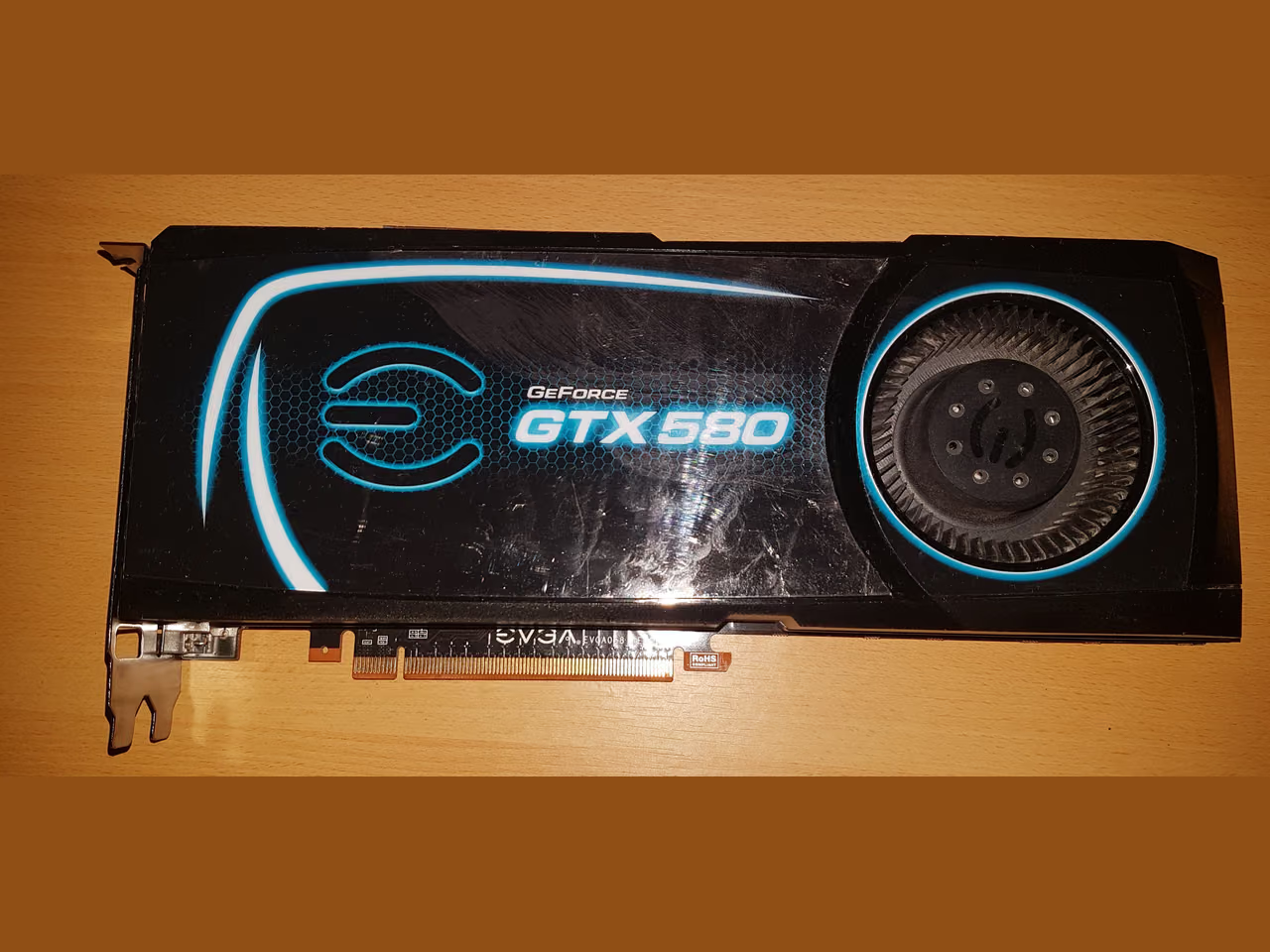
About this machine

NVIDIA's surviving launch table supplies clocks, memory and bandwidth. It does not state an explicitly labelled FP32 peak or a numeric board-power rating.

Configuration

Reference card

Component Role Count Clock Capacity
NVIDIA Fermi (NVIDIA GeForce GTX 580) Reference-card graphics clock. GPU 1 772 MHz Nominal clock
NVIDIA GeForce GTX 580 frame buffer Video memory 1 1536 MiB

Figures for the whole machine

NVIDIA GeForce GTX 580: system figures

provisional A figure marked provisional is recorded but not accepted: its evidence is unsettled. It may rely on one source, an unconfirmed announcement, or a digit read from a damaged scan. The reason appears under the figure. The catalog shows the figure but never uses it in a multiplier. How records are judged.

Metric Value Evidence Basis Method Source
Memory bandwidth whole-system provisional 192.4 GB/s Confirmed Derived Theoretical peak Computed here from figures the vendor stated Adds the one fitted frame-buffer bandwidth. No host memory is included.

Figures for its components

NVIDIA Fermi (NVIDIA GeForce GTX 580)

provisional A figure marked provisional is recorded but not accepted: its evidence is unsettled. It may rely on one source, an unconfirmed announcement, or a digit read from a damaged scan. The reason appears under the figure. The catalog shows the figure but never uses it in a multiplier. How records are judged.

Metric Value Evidence Basis Method Source
Clock frequency gpu provisional 772 MHz Confirmed Vendor-rated Nominal clock Stated by the vendor The reference-card graphics clock.
Thermal design power gpu provisional 243 W Rumored Vendor-rated Rated power From community documentation Nvidia's own material for this chip states no thermal figure. Wikipedia gives 243 W as the card's rated thermal design power, and the catalog carries it as rumored.
1 documented absence
NVIDIA Fermi (NVIDIA GeForce GTX 580): documented absences
Metric Value Evidence Basis Method Source
Peak FP32 rate gpu provisional unknown The launch table gives CUDA-core and processor-clock figures, but no explicitly labelled single-precision throughput. Not stated Theoretical Theoretical peak Stated by the vendor The recovered NVIDIA launch material does not state an explicitly labelled FP32 peak.
NVIDIA GeForce GTX 580 frame buffer

provisional A figure marked provisional is recorded but not accepted: its evidence is unsettled. It may rely on one source, an unconfirmed announcement, or a digit read from a damaged scan. The reason appears under the figure. The catalog shows the figure but never uses it in a multiplier. How records are judged.

Metric Value Evidence Basis Method Source
Memory bandwidth memory provisional 192.4 GB/s Confirmed Theoretical Theoretical peak Stated by the vendor Vendor-stated maximum transfer rate of this memory interface, not a benchmarked application result.
Memory capacity whole-system provisional 1536 MiB Confirmed Vendor-rated Design capacity Stated by the vendor The frame buffer fitted to the reference accelerator; host memory is excluded.

Derived figures and comparisons

Computed by this project rather than read from a source, and recomputed from their inputs on every build.

192 400 000 000 B/s

Formula
a + b + … sum v1
Inputs
  • nvidia-geforce-gtx-580-memory Memory bandwidth: 192.4 GB/s
Rounding
none , 12 significant digits

Adds 1 memory-bandwidth figure obtained by theoretical-peak. Nothing in the catalog is left out of it. A total is only as trustworthy as the decision about what belongs in it, so both the terms and the exclusions are named records.

Editorial notes

This accelerator’s whole-system memory is its fitted frame buffer; host memory is excluded. Partner cards may differ from this reference configuration.

Sources

Back to top